IC Specification
The StarFive JH7110 LCD module uses Cadence IP. The following is the information about Cadence IP.
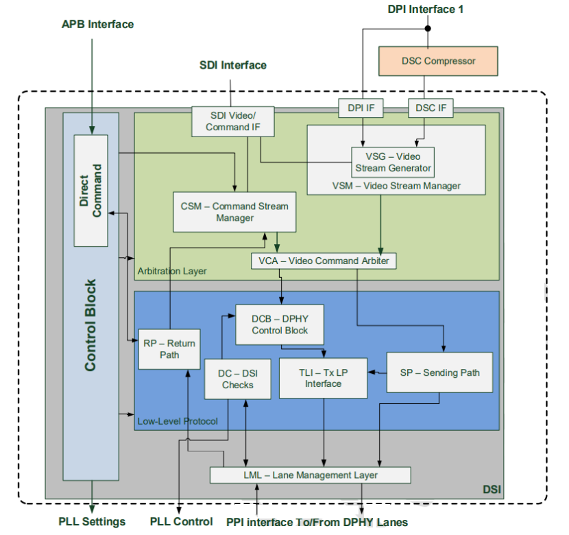
MIPI DSITX CADENCE
The Cadence MIPI DSI v1.3.1 TX Controller IP (DSITX) provides an interface that receives data and control from the host processor display system using either the DPI, DSC or SDI input bus interfaces. The DSITX will translate the incoming pixel information and control signals into an internal packed byte format, in the case of DPI and DSC, or pass in the pre-packed SDI byte format, before the internal byte format data is packeted and sent to the MIPI DSI Compatible display via the D-PHY physical interface. It supports video and command mode displays and can work in dual-display mode using virtual channel identification on the packets.
The supported MIPI display types are (at least) type 1 (command only), type 2 (video plus a partial-frame buffer in command mode), type 3 (video display with some programming capability in command mode).
In video mode, all the regular modes are supported (Non-Burst with Sync Pulses, Non-Burst with Sync Events and same for Burst mode).
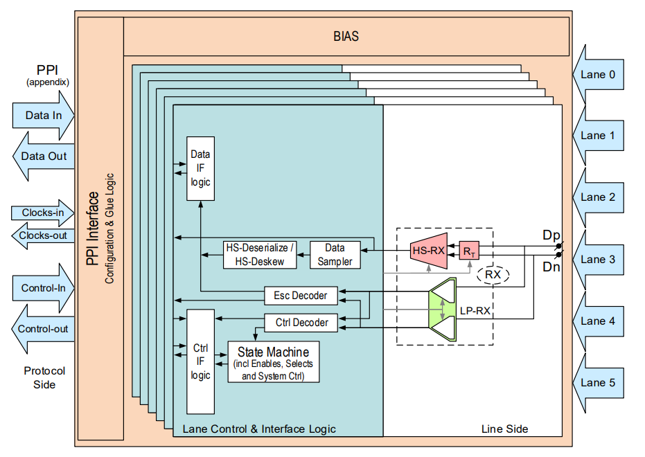
MIPI DPHY M31
- Supports standard 8b PPI interface compliant of MIPI D-PHY Specification.
- Supports 1 Clock Lane and up to 4 Data Lanes scalability in DPHY mode.
- Supports independent (1 Clock Lane & up to 2 Data Lanes) X 2 in DPHY mode.
- Supports HS-Rx Data rate from 80Mbps up to 1.5 Gbps. (DPHY)
- Supports LS-Rx Data rate of 10Mbps & Ultra-low power mode.
- Supports Triggers, ULPS and LPDT.
- Supports on-die terminated and non-terminated operation, integrates switchable termination.
- Supports Fault Detection of Sequence Error. (Error Report)
- Supports clock and data lane swapping function.
- Build-in BISTTX for at-speed testing.
IP Overview