DDR Interface and Timing
DDR4/DDR3
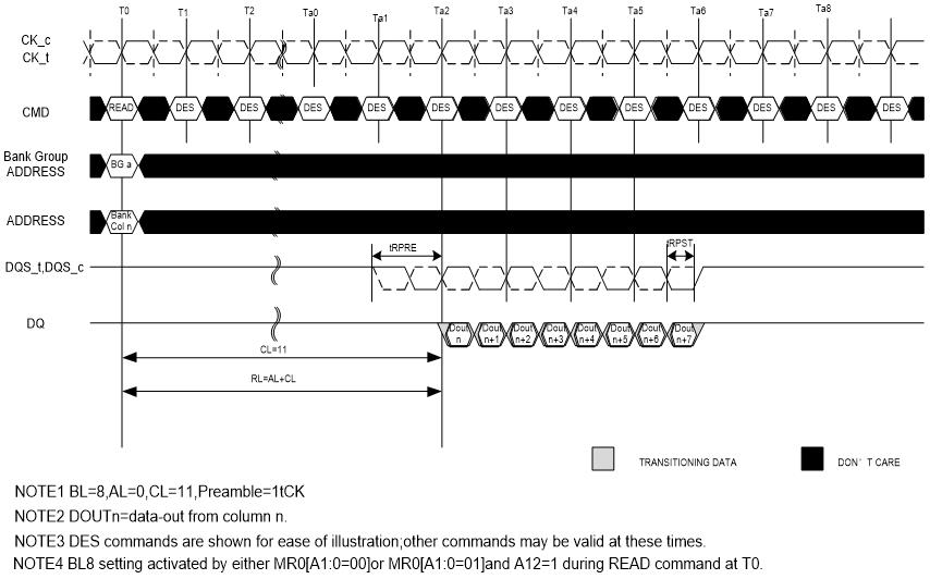
READ Burst Operation RL=11(AL=0, CL=11, BL8)
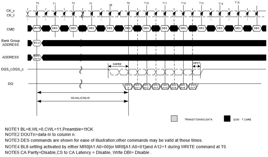
WRITE Burst Operation WL=9(AL=0, CWL=9, BL8)
LPDDR4
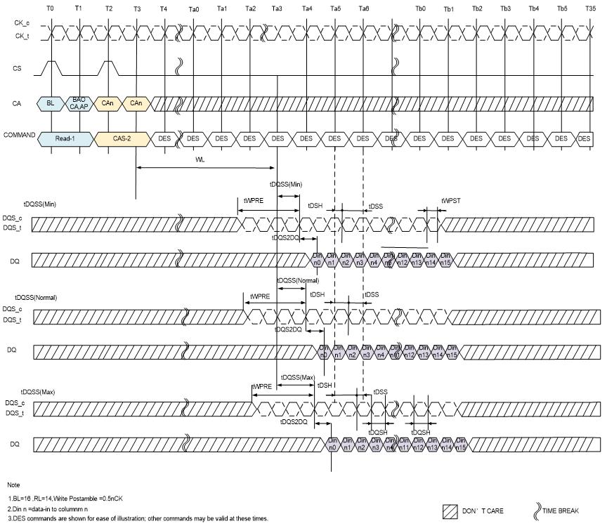
Burst Read

Burst Write
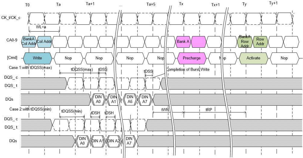
LPDDR3
Burst Read: RL=12, BL=8, tDQSCK > tCK

Burst Write