Electrical Specification
Power Supply
Power-up Sequence
JH-7110 has 3 power supplies, VDD, AVDL, and AVDH. VDD and AVDL are both core power supplies and while separate pins are used for noise isolation purposes.
The recommended power sequence is that from digital core voltage to analog I/O voltage and from low voltage level to high voltage level. This is not considered a constraint, but instead, a guideline, as it could result in the best-case operating scenario, where the leakage currents during power up are kept to a minimum.
| Recommended Merge Net | Ball Name |
|---|---|
| VDD18_AON |
|
|
VDD09_CPU VDD09_AON |
|
|
VCC18A_MIPITX VCC18A_MIPIRX VDD18 VDDQ11 |
|
|
VDD_MIPITX VCCO9A_MIPIRX VDD09 |
|
| VDD18/VDD33 |
|
| PAD_RSTN | PAD_RSTN |
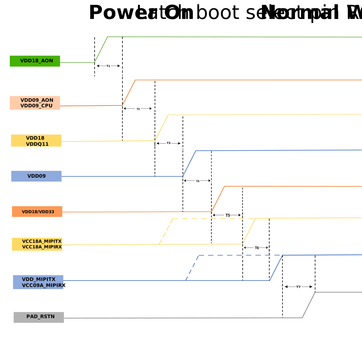
- VCC18A_MIPITX and VCC18A_MIPIRX can power up at T3; VDD_MIPITX and VCC09A_MIPIRX can power up at T4.
- VCC18A_MIPITX and VCC18A_MIPIRX can power up at T6; VDD_MIPITX and VCC09A_MIPIRX can power up at T7. (Default in the solution)
- VCC18A_MIPITX and VCC18A_MIPIRX can power up after reset; VDD_MIPITX and VCC09A_MIPIRX can power up after reset; CC18A_MIPITX and VCC18A_MIPIRX must before VDD_MIPITX and VCC09A_MIPIRX;
| Sequence | Interval |
|---|---|
| T1 | 1ms |
| T2 | 1ms |
| T3 | 1ms |
| T4 | 1ms |
| T5 | 1ms |
| T6 | 1ms |
| T7 | 64ms |
Power Pin Voltage
| Power Pin in PMIC | Package Ball Name | Power Pin Index | Voltage (V) | Comment |
|---|---|---|---|---|
| VDD09_AON | VDD | 1 | 0.9 | Standby mode, all AON relevant power supplies should be on and all others off. |
| VDD_RTC | ||||
| VDD09_CPU | VDD_CPU | 2 | 0.9 to 1.0 | CPU core power supply, which can be adjusted to 1.0 V |
| VDD18_AON | VDD18_OSC | 3 | 1.8 | AON domain GPIO, RPIO,RESETN,TESTEN,1.8 V only |
| VDD18_OTP | ||||
| VDD1833_AON | ||||
| VDD1825_GMAC0 | VDD1825_GMAC0 | 4 | 1.8/2.5 | IO voltage for GMAC0, 1.8 V and 2.5 V switchable, AON domain |
| VDD18_HDMI | AVDD_HDMI | 5 | 1.8 | HDMI and MIPITX 1.8 V analog power supply which should be powered on first |
| VDD09_HDMI | AVDD09_HDMI | 6 | 0.9 | The 0.9 V voltage for Core, PLL, MIPI, and so on, should be powered on after VDD18_HDMI_MIPITX. VDD09_HDMI should be powered on together with VOUT digital. |
| PVDD_HDMI | ||||
| VDD18_MIPITX | VCC18A_MIPITX | 7 | 1.8 | |
| VDD09_MIPITX | VDD_MIPITX | 8 | 0.9 | |
| VDD18_MIPIRX | VCC18A_MIPIRX | 9 | 1.8 | MIPI RX 1.8 V analog power supply which should be powered on first |
| VDD09_MIPIRX | VCC09A_MIPIRX | 10 | 0.9 | MIPI RX 0.9 V power supply, which should be powered on after VDD18_MIPIRX |
| VDD33_USB2 | VCCA33_USB | 11 | 3.3 | 3.3 V USB interface voltage, which should be powered on after the 1.8 V and 0.9 V voltage, and powered off first. |
| VDD09_TOP | AVDD09_USB | 12 | 0.9 | |
| AVDL_PCIE0 | ||||
| AVDL_PCIE1 | ||||
| VDD_PLL0 | ||||
| VDD_PLL1 | ||||
| VDD_PLL2 | ||||
| VDD_DDR | DDR PHY core power 0.9 V | |||
| VDDPLL_DDR | DDR PHY PLL power 0.9 V | |||
| VDD18_TOP | VCCA18_PLL0 | 13 | 1.8 | |
| VCCA18_PLL1 | ||||
| VDD18_TEMP | ||||
| VDDA18_TEMP | ||||
| VCCA18_PLL2 | ||||
| AVDH_PCIE0 | ||||
| AVDH_PCIE1 | ||||
| VCCA18_USB | ||||
| VDDQ11_DDR | VDDQ_DDR | 14 | 1.1 | DDR PHY IO and clock IO voltage, 1.1 V |
| VDDQCK_DDR | ||||
| VDD1833_GPIO1 | VDD1833_GPIO1 | 15 | 1.8/3.3 | GPIO Group 1 voltage, 1.8 V and 3.3 V switchable |
| VDD1833_GPIO2 | VDD1833_GPIO2 | GPIO Group 2 voltage, 1.8 V and 3.3 V switchable | ||
| VDD1833_GPIO3 | VDD1833_GPIO3 | GPIO Group 3 voltage, 1.8 V and 3.3 V switchable | ||
| VDD1833_GPIO4 | VDD1833_GPIO4 | 16 | GPIO Group 4 voltage, 1.8 V and 3.3 V switchable | |
| VDD1833_SD0 | VDD1833_SD0 | SD0 IO voltage, 1.8 V and 3.3 V switchable | ||
| VDD1833_QSPI | VDD1833_QSPI | 16 | 1.8/3.3 | QSPI IO voltage, 1.8 V and 3.3 V switchable |
| VDD1825_GMAC1 | VDD1825_GMAC1 | 17 | 1.8/2.5 | GMAC IO voltage, 1.8 V and 2.5 V switchable |
Power Group
| Group | Name | Dir | Description |
|---|---|---|---|
| Analog P/G | AVDH | PAD | 1.8 V analog power supply |
| AVDL | PAD | 0.9 V analog power supply | |
| AVSS | PAD | Analog ground | |
| High-Speed Signal | RXP | PAD | Differential data input of RX, positive |
| RXN | PAD | Differential data input of RX, negative | |
| TXP | PAD | Differential data output of TX, positive | |
| TXN | PAD | Differential data output of TX, negative | |
| Reference Clock Input/Output | CKREFP | PAD | Differential pair that can be configured as either a reference clock input or a reference clock output, P for positive and N for negative. |
| CKREFN | PAD | ||
| Digital P/G | VDD/VDDA/VDDB | PIN |
VDD/VSS – Digital Power from the core inside. VDDA/VDDB/VSSA/VSSB – PIN of Power Cut IO between Analog Power Domain and Digital Power Domain. |
| VSS/VSSA/VSSB | PIN |
Absolute Maximum Ratings
Absolute Maximum Ratings are values beyond which damage to the device may occur. The following table specifies the absolute maximum ratings over the operating junction temperature range of commercial and extended temperature devices. Functional operation of the device at these or any other conditions beyond those indicated in the operational sections of this standard may damage the device.
| Symbol | Parameters | Min | Max | Units |
|---|---|---|---|---|
| VDD | Power supply for Core | 0.81 | 0.99 | V |
| VDDIO | Power supply for Post-Driver | -0.5 | 3.63 | V |
| Tj | junction temperature range | -20 | 125 | ℃ |
| Ts | Recommended storage condition | -20 | 125 | ℃ |
| Ta | Ambient operating temperature | -20 | 85 | ℃ |
- The storage temperature range applies when the device is in the OFF state (the device is not assembled in any platform and is not electrically connected to any voltage or I/O signals). Damage may occur when the device is subjected to this temperature for any length of time.
- For devices shipped in tape and reel, the storage temperature range is [+20°C~26°C] and relative humidity (RH) range is [40%~60%]. StarFive recommends allowing the device to return to ambient room temperature before usage.
Recommended Operating Conditions
| Power Pin | Ground | Description | Min | Typ | Max | Unit | |
|---|---|---|---|---|---|---|---|
| VDD | VSS | Core power supply | 0.81 | 0.9 | 0.99 | V | |
| VDD18 | Digital IO power supply | 1.62 | 1.8 | 1.98 | V | ||
| VDD33 | Digital function IO power supply | 3.135 | 3.3 | 3.465 | V | ||
| AVDD18_MIPITX | VSS | MIPI TX analog power supply | 1.62 | 1.8 | 1.98 | V | |
| AVDD18_MIPIRX | AVSS_MIPIRX | MIPI RX analog power supply for LDO | 1.62 | 1.8 | 1.98 | V | |
| AVDD09_MIPIRX | MIPI RX analog power supply | 0.855 | 0.9 | 0.99 | V | ||
| AVDD18_TS | VSS18_TS | Temperature sensor analog power supply | 1.62 | 1.8 | 1.98 | V | |
| AVDD33_USB | AVSS_USB | USB analog power supply | 2.97 | 3.3 | 3.63 | V | |
| AVDD18_USB | USB analog power supply | 1.62 | 1.8 | 1.98 | V | ||
| AVDD18_PCIE | AVSS_PCIE | USB TX analog power supply | 1.62 | 1.8 | 1.98 | V | |
| AVDD09TX_PCIE | AVSS09TX_PCIE | PCIE TX analog power supply | 0.85 | 0.9 | 0.95 | V | |
| AVDD09RX_PCIE | AVSS09RX_PCIE | PCIE RX analog power supply | 0.85 | 0.9 | 0.95 | V | |
| AVDD18_HDMI | AVSS18_HDMI | HDMI analog power supply | 1.62 | 1.8 | 1.98 | V | |
| AVDD09P_HDMI | AVSS09P_HDMI | HDMI analog power supply of PLL | 0.81 | 0.9 | 0.99 | V | |
| AVDD09D_HDMI | AVSS09D_HDMI | HDMI analog power supply of data channel | 0.81 | 0.9 | 0.99 | V | |
| DVDD18_OTP | VSS18_OTP | OTP power supply | 1.62 | 1.8 | 1.98 | V | |
| AVDD09_PLL0 | AVSS_PLL0 | PLL0 analog power supply | 0.81 | 0.9 | 0.99 | V | |
| AVDD09_PLL1 | AVSS_PLL1 | PLL1 analog power supply | 0.81 | 0.9 | 0.99 | V | |
| AVDD09_PLL2 | AVSS_PLL2 | PLL2 analog power supply | 0.81 | 0.9 | 0.99 | V | |
| DDR4/LPDDR4 | VDDPLL_DDR0 | VSS | DDR0 PLL power supply | 0.81 | 0.9 | 0.99 | V |
| VDDQ_DDR0 | DDR0 IO power supply | 1.14/1.06 | 1.2/1.1 | 1.26/1.17 | V | ||
| VDDQCK_DDR0 | DDR0 CK power supply | 1.14/1.06 | 1.2/1.1 | 1.26/1.17 | V | ||
| DDR3/LPDDR3 | VDDPLL_DDR0 | VSS | DDR0 PLL power supply | 0.81 | 0.9 | 0.99 | V |
| VDDQ_DDR0 | DDR0 IO power supply | 1.425/1.14 | 1.5/1.2 | 1.575/1.3 | V | ||
| VDDQCK_DDR0 | DDR0 CK power supply | 1.425/1.14 | 1.5/1.2 | 1.575/1.3 | V | ||
- Power supply voltage beyond operating range is not guaranteed.
- Power/Ground bouncing beyond DC operating range may cause invalid data output. It is not guaranteed by eMemory and customers must ensure power stability on their own.
- Normally operating junction temperature is from -20 ℃ to 125 ℃ and program operations should be at junction temperature -20 ℃ to 125 ℃.
Static Power Consumption
The static power consumption of JH-7110 is 130 mW.
DC Electrical Characteristics
| Symbol | Parameter | Min | Typ | Max | Unit |
|---|---|---|---|---|---|
| VIL | Input Low-Level Voltage | -0.3 | - | 0.35 × VDDIO | V |
| VIH | Input High-Level Voltage | 0.65 × VDDIO | - | VDDIO + 0.3 | V |
| VT+ | Hysteresis Threshold up | 0.4 × VDDIO | - | 0.7 × VDDIO | V |
| VT- | Hysteresis Threshold down | 0.3 × VDDIO | - | 0.6 × VDDIO | V |
| Vhys | Input Hysteresis Voltage | 0.1 × VDDIO | - | 0.4 × VDDIO | V |
| Rpu | Pull-up Resistor | Ω | |||
| Rpd | Pull-down Resistor | Ω | |||
| VOL | Output Low-Level Voltage | - | - | 0.45 | V |
| VOH | Output High-Level Voltage | 1.35 | - | - | V |
| IOL | Low Level Output Current @VOL (Max) | ||||
| Drive Strength (E2, E1=00) | 3.3 | 4.9 | 8.8 | mA | |
| Drive Strength (E2, E1=01) | 7.7 | 11.5 | 20.5 | mA | |
| Drive Strength (E2, E1=10) | 13.2 | 19.7 | 35.0 | mA | |
| Drive Strength (E2, E1=11) | 17.6 | 26.2 | 46.7 | mA | |
| IOH | High-Level Output Current @VOH (Min) | ||||
| Drive Strength (E2, E1=00) | 3.6 | 5 | 7.7 | mA | |
| Drive Strength (E2, E1=01) | 7.1 | 10 | 15.4 | mA | |
| Drive Strength (E2, E1=10) | 13.1 | 18.3 | 28.3 | mA | |
| Drive Strength (E2, E1=11) | 16.6 | 23.2 | 36.0 | mA |
| Symbol | Parameter | Min | Typ | Max | Unit |
|---|---|---|---|---|---|
| VIL | Input Low Level Voltage | -0.3 | - | 0.7 | V |
| VIH | Input High Level Voltage | 1.7 | - | VDDIO + 0.3 | V |
| VT+ | Hysteresis Threshold up | 0.9 | - | 1.7 | V |
| VT- | Hysteresis Threshold down | 0.7 | - | 1.5 | V |
| Vhys | Input Hysteresis Voltage | 0.2 | - | 1.0 | V |
| Rpu | Pull-up Resistor | Ω | |||
| Rpd | Pull-down Resistor | Ω | |||
| VOL | Output Low-Level Voltage | - | - | V | |
| VOH | Output High-Level Voltage | - | - | V | |
| IOL | Low Level Output Current @VOL (Max) | ||||
| Drive Strength (E2, E1=00) | 3.7 | 5.3 | 9.1 | mA | |
| Drive Strength (E2, E1=01) | 8.5 | 12.3 | 21.1 | mA | |
| Drive Strength (E2, E1=10) | 14.5 | 21.0 | 36.2 | mA | |
| Drive Strength (E2, E1=11) | 19.3 | 28.0 | 48.3 | mA | |
| IOH | High-Level Output Current @VOH (Min) | ||||
| Drive Strength (E2, E1=00) | 4.1 | 5.1 | 7.8 | mA | |
| Drive Strength (E2, E1=01) | 8.0 | 10.2 | 15.7 | mA | |
| Drive Strength (E2, E1=10) | 13.1 | 18.6 | 28.7 | mA | |
| Drive Strength (E2, E1=11) | 16.7 | 23.7 | 36.6 | mA |
| Symbol | Parameter | Min | Typ | Max | Unit |
|---|---|---|---|---|---|
| VIL | Input Low Level Voltage | -0.3 | - | 0.8 | V |
| VIH | Input High Level Voltage | 2 | - | VDDIO + 0.3 | V |
| VT+ | Hysteresis Threshold up | 0.9 | - | 2.1 | V |
| VT- | Hysteresis Threshold down | 0.7 | - | 1.9 | V |
| Vhys | Input Hysteresis Voltage | 0.2 | - | 1.4 | V |
| Rpu | Pull-up Resistor | Ω | |||
| Rpd | Pull-down Resistor | Ω | |||
| VOL | Output Low-Level Voltage | - | - | V | |
| VOH | Output High-Level Voltage | - | - | V | |
| IOL | Low Level Output Current @VOL (Max) | ||||
| Drive Strength (E2, E1=00) | 3.4 | 5.0 | 8.5 | mA | |
| Drive Strength (E2, E1=01) | 8.0 | 11.6 | 19.7 | mA | |
| Drive Strength (E2, E1=10) | 13.6 | 19.8 | 33.8 | mA | |
| Drive Strength (E2, E1=11) | 18.1 | 26.4 | 45.1 | mA | |
| IOH | High-Level Output Current @VOH (Min) | ||||
| Drive Strength (E2, E1=00) | 3.3 | 4.8 | 7.5 | mA | |
| Drive Strength (E2, E1=01) | 6.6 | 9.5 | 15.0 | mA | |
| Drive Strength (E2, E1=10) | 12.2 | 17.4 | 27.5 | mA | |
| Drive Strength (E2, E1=11) | 15.5 | 22.1 | 34.7 | mA |
Maximum Current Consumption
| Type | Power | Ground | Attribute | Voltage (V) | Current (mA) | Description | ||||
|---|---|---|---|---|---|---|---|---|---|---|
| Min | Typ | Max | Min | Typ | Max | |||||
| CORE | VDD | VSS | AON | 0.81 | 0.9 | 0.99 | 10 | 900 | 1,000 | Core power supply for AON modules and the top layer |
| VDD_CPU | VSS | AON | 0.9 | 0.9 | 1 | 1,000 | 2,000 | CPU power supply, which could be up-scaled to 1.0V | ||
| GPIO | VDD1825_GMAC1 | VSS | 1.62/2.25 | 1.8/2.5 | 1.98/2.75 | - | 4 | 20 | ||
| VDD1825_GMAC0 | VSS | AON | 1.62/2.25 | 1.8/2.5 | 1.98/2.75 | - | 4 | 20 | GMAC0 is in AON | |
| VDD1833_AON | VSS | AON | 1.62 | 1.8 | 1.98 | - | 4 | 20 | The AON RGPIO is 1.8V only | |
| VDD1833_GPIO1 | VSS | 1.62/2.97 | 1.8/3.3 | 1.98/3.63 | - | 4 | 20 | |||
| VDD1833_GPIO2 | VSS | 1.62/2.97 | 1.8/3.3 | 1.98/3.63 | - | 4 | 20 | |||
| VDD1833_GPIO3 | VSS | 1.62/2.97 | 1.8/3.3 | 1.98/3.63 | - | 4 | 20 | |||
| VDD1833_GPIO4 | VSS | 1.62/2.97 | 1.8/3.3 | 1.98/3.63 | - | 4 | 20 | |||
| SD0/eMMC | VDD1833_SD0 | VSS | 1.62/2.97 | 1.8/3.3 | 1.98/3.63 | - | 4 | 20 | ||
| QSPI | VDD1833_QSPI | VSS | 1.62/2.97 | 1.8/3.3 | 1.98/3.63 | - | 4 | 20 | ||
| PLL | VDD_PLL0 | VSS_PLL0 | 0.81 | 0.9 | 0.99 | - | - | 5 | PLL analog power supply | |
| VDD_PLL1 | VSS_PLL1 | 0.81 | 0.9 | 0.99 | - | - | 5 | PLL analog power supply | ||
| VDD_PLL2 | VSS_PLL2 | 0.81 | 0.9 | 0.99 | - | - | 5 | PLL analog power supply | ||
| VCCA18_PLL0 | VSS_PLL0 | 1.62 | 1.8 | 1.98 | - | - | 10 | PLL analog power supply | ||
| VCCA18_PLL1 | VSS_PLL1 | 1.62 | 1.8 | 1.98 | - | - | 10 | PLL analog power supply | ||
| VCCA18_PLL2 | VSS_PLL2 | 1.62 | 1.8 | 1.98 | - | - | 10 | PLL analog power supply | ||
| OSC | VDD_RTC | VSS_RTC | AON | 0.81 | 0.9 | 0.99 | - | - | 2.5 | |
| VDD18_OSC | VSS18_OSC | AON | 1.62 | 1.8 | 1.98 | - | 4 | 4 | ||
| OTP | VDD18_OTP | VSS18_OTP | AON | 1.62 | 1.8 | 1.98 | - | 4 | 4 | |
| LPDDR4 | VDDPLL_DDR | VSS | 0.81 | 0.9 | 0.99 | - | 10 | 100 | DDR PLL power supply | |
| VDDQ_DDR | VSS | 1.14/1.06 | 1.2/1.1 | 1.26/1.17 | - | 200 | 800 | VDDQ DDR IO power supply | ||
| VDDQCK_DDR | VSS | 1.14/1.06 | 1.2/1.1 | 1.26/1.17 | - | 64 | 200 | DDR CK power supply | ||
| VDD_DDR | VSS | 0.81 | 0.9 | 0.99 | - | 10 | 600 | Net name of VDD_DDR is the core power supply for DDR PHY | ||
| HDMI | AVDD_HDMI | AVSS_HDMI | 1.62 | 1.8 | 1.98 | - | 20 | 40 | ||
| AVDD09_HDMI | AVSS_HDMI | 0.81 | 0.9 | 0.99 | - | 12 | 40 | |||
| PVDD_HDMI | PVSS_HDMI | 0.81 | 0.9 | 0.99 | - | 8 | 150 | |||
| USB | AVDD09_USB | AVSS_USB | 0.81 | 0.9 | 0.99 | - | 12 | 18 | ||
| VCCA18_USB | AVSS_USB | 1.62 | 1.8 | 1.98 | - | 9 | 20 | |||
| VCCA33_USB | AVSS_USB | 2.97 | 3.3 | 3.63 | - | 5 | 20 | |||
| Temp Sensor | VDD18_TEMP | VSS18_TEMP | 1.62 | 1.8 | 1.98 | - | 2 | 12 | ||
| VDDA18_TEMP | VSS18_TEMP | 1.62 | 1.8 | 1.98 | - | 2 | 20 | |||
| PCIE | AVDH_PCIE0 | AVSS_PCIE0 | 1.62 | 1.8 | 1.98 | - | 20 | 40 | ||
| AVDL_PCIE0 | AVSS_PCIE0 | 0.81 | 0.9 | 0.99 | - | 12 | 40 | |||
| AVDH_PCIE1 | AVSS_PCIE1 | 1.62 | 1.8 | 1.98 | - | 20 | 40 | |||
| AVDL_PCIE1 | AVSS_PCIE1 | 0.81 | 0.9 | 0.99 | - | 12 | 40 | |||
| MIPI RX | VCC09A_MIPIRX | GND09A_MIPIRX | 0.855 | 0.9 | 0.99 | - | 4.5 | 40 | ||
| VCC18A_MIPIRX | GND09A_MIPIRX | 1.62 | 1.8 | 1.98 | - | 8 | 40 | |||
| MIPI TX | VDD_MIPITX | VSS | 0.855 | 0.9 | 0.99 | - | 4.5 | 40 | ||
| VCC18A_MIPITX | VSS_MIPITX | 1.62 | 1.8 | 1.98 | - | 8 | 40 | |||