Block Diagram
The block diagram of the display subsystem is displayed in following diagram.
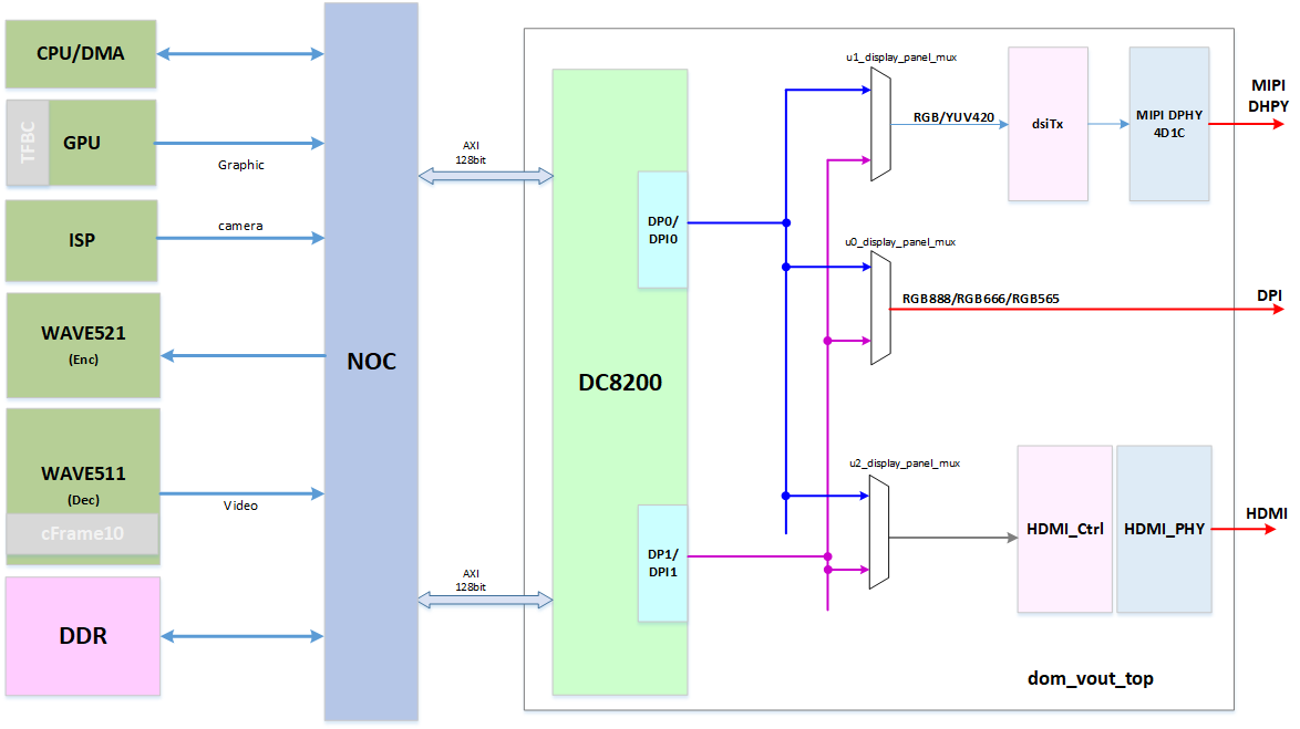
Data Mapping
The DSI transmitter's pixel data could be from panel 0 or panel 1 interface of DC8200, and could be selected from DP or DPI interface. The RGB PAD and HDMI have similar mechanism.
| Destination | Supported Data Mapping | Comment |
|---|---|---|
| DPI to PAD |
|
For flexibility |
| DSI Tx Data from DC8200 |
|
Default DPI |
| HDMI Data from DC8200 |
|
DP by default, and DPI for backup |