DDR PHY
The DDR PHY of JH-7110 has the following analog power characteristics.
- All power outputs are generated from bump.
- PHY switch off the power supply only in sleep mode.
- Before entering the sleep mode, CPU will turn off the PHY power supply via board level switch.
Note the following for DDR PHY power integration. Figure 1. DDR PHY Power Diagram
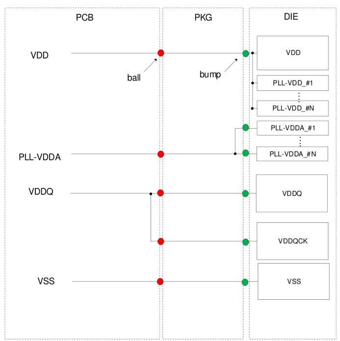
- The SoC VSS can be short with PHY VSS in die by connecting the SoC and PHY VSS bump together using AP RDL layer.
- PHY VDD cannot be short with SoC VDD in die.
- You can short the PHY VDD with SoC VDD at package or PCB level as long as VDD noise target is met.