The PCIE Multi-Purpose PHY of JH-7110 has the following analog power characteristics.
Provide AVDH/AVDL pad output
Independent VDD pad output
Controlled on the board level.
Power Up Sequence
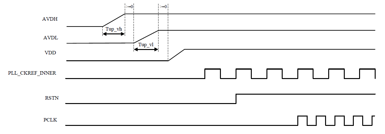
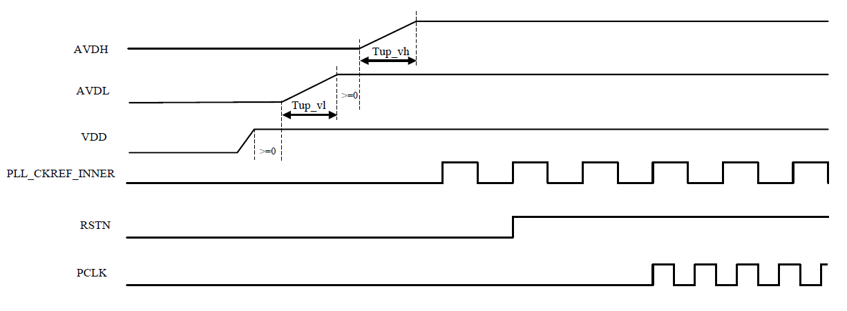
The PHY has three power supplies, VDD, AVDL and AVDH. VDD and AVDL are both Core
Power supplies and while separate pins are used for noise isolation purposes. AVDH
is the IO Power supply.Figure 1. PCIE Power-Up Sequence 1 (AVDH→AVDL→VDD or AVDH→VDD→AVDL )Figure 2. PCIE Power-Up Sequence 2(VDD→AVDL→AVDH or AVDL→VDD→AVDH )
Table 1. PCIE Power-on Time Information
Symbol
Parameter
Min
Typ
Max
Unit
Tup_vh
The power-on time of AVDH
0.3
ms
Tup_vl
The power-on time of AVDL
0.5
ms
Note: If the power-on time of AVDL or AVDH is too
short, there may be large pulse current during the power on process, the maximum
of pulse current may be greater than 400mA when the power-on time is
100us.
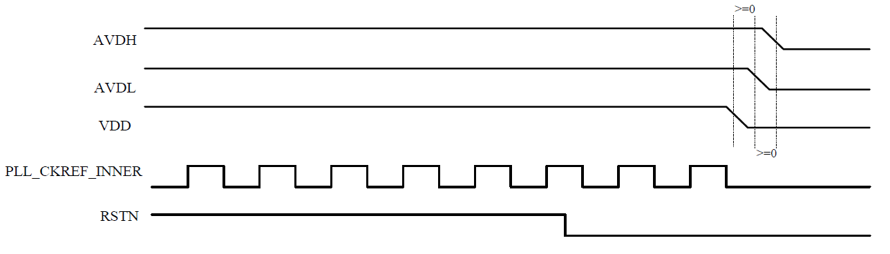
Power Down Sequence
The PHY has three power supplies,VDD, AVDL and AVDH.VDD and AVDL are both Core Power
supplies and while separate pins are used for noise isolation purposes. AVDH is the
IO Power supply.Figure 3. PCIE Power Down Sequence
Table 2. PCIE IO PAD
Group
Name
Dir
#
Description
Analog P/G
AVDH
PAD
*
1.8Vanalog power supply
AVDL
PAD
*
0.9Vanalog power supply
AVSS
PAD
*
analog ground
High Speed signal
RXP
PAD
1
differential data input of RX, positive
RXN
PAD
1
differential data input of RX, negative
TXP
PAD
1
differential data output of TX, positive
TXN
PAD
1
differential data output of TX, negative
Reference Clock input/output
CKREFP
PAD
1
Differential pair that can be configured as
either a reference clock input or a reference clock
output.
CKREF_SRC[1:0]=01:
CKREFP/N are used as
input reference clock source
CKREF_SRC[1:0]=10:
CKREFP/N are used as output clock
to supply a differential 100M reference clock. See PCIE Reference Clock Input/Output for more information.
Note: CKREFP/N is valid means
CKREFP/N can output 100MHz differential
clock.
CKREFN
PAD
1
Digital P/G
VDD/VDDA/VDDB
PIN
VDD/VSS –Digital Power from core
side.
VDDA/VDDB/VSSA/VSSB –PIN of Power Cut IO between
Analog Power Domain and Digital Power Domain