The MIPI transceiver of JH-7110 has
the following analog power characteristics.
VCC09D and VCC18A are independent pad outputs.
VCC18A and VCC09D are controlled on the board level.
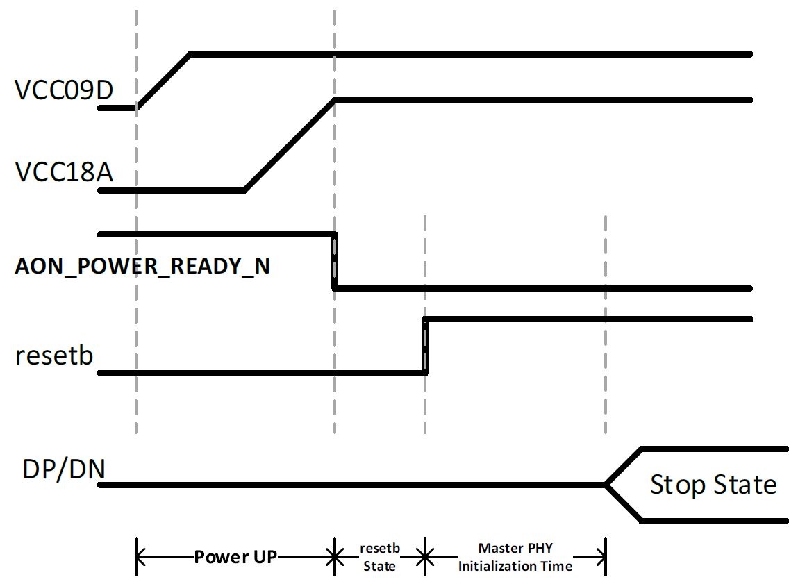
Figure 1. MIPI TX Power Up Timing
The recommended power up sequence is that from digital core voltage to analog I/O voltage
and from low voltage level to high voltage level. This is not considered as a
constraint, but a guideline instead, as it results in the best-case operating scenario,
where the leakage currents during powering up are kept to a minimum.
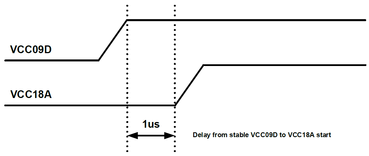
For keeping leakage current during power up to a minimum, the powering up sequence
guideline would be from digital core voltage to analog I/O voltage and from low voltage
level to high voltage level. There are 2 power domains in M31DPHYTX512TL028D, which are
VCC09D and VCC18A. The VCC09D is 0.9V supplies, and VCC18A is 1.8V. So, the recommended
powering up sequence for this IP is to power up VCC09D first, and then power up VCC18A
at the following.Figure 2. MIPI TX Power Up Sequence
Table 1. MIPI TX Analog Pad and Power/Ground
Pin Name
Direction
With PAD
Description
VCC09D
Input
No
0.9V digital supply voltage that connects to the core power.
GND09D
Input
No
Digital ground supply that connects to the core power.
VCC18A
Input
Yes
1.8V analog supply voltage for the DPHY analog part.