The MIPI receiver of JH-7110 has the
following analog power characteristics.
VCC09D is a independent pad output.
VCC18A/VCC09A generates output from the system pad.
VCC18A/VCC09A and VCC09D are controlled on the board level.
Power and Ground
The following table provides the power and ground information.
Table 1. MIPI RX Analog and Digital Power Supplies
Name
Value
Description
VCC09A
0.9V (-5% + 10% with respect to GNDA)
0.9 V analog supply with pad.
VCC09D
0.9V (±10% with respect to GND09D)
0.9 V digital supply.
VCC18A
1.8V (±10% with respect to GNDA)
1.8 V analog supply with pad.
The analog power supplies should be isolated from the power supplies of the ASIC to
prevent extra jitter caused by the unexpected noise. As to the VCC09D andGND09D, it
is permitted to share with the core power of the ASIC. In addition, the power/ground
connection should provide a robust and low-impedance plane for ESD protection.
Table 2. MIPI RX Analog Pad and Power/Ground
Pin Name
Direction
With PAD
Description
VCC09D
Input
No
0.9 V digital supply voltage that connects to the core
power.
GND09D
Input
No
Digital ground supply that connects to the core
power.
VCC09A
Input
Yes
0.9 V analog supply voltage. 1uF external capacitor is
needed.
VCC18A
Input
Yes
1.8 V analog supply voltage. 1uF external capacitor is
needed.
GNDA
Input
Yes
Analog ground supply for the analog part.
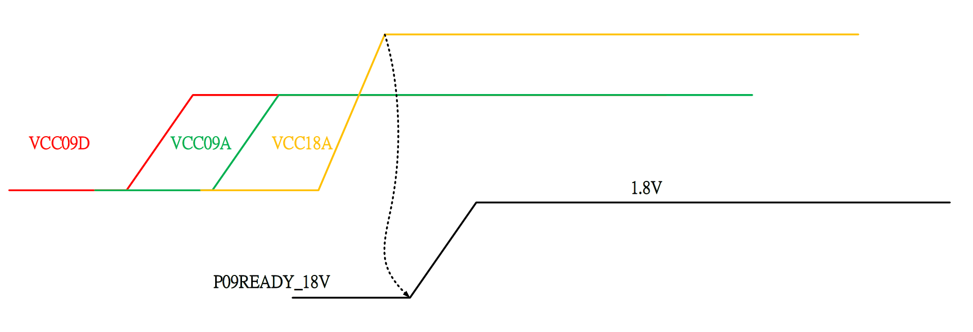
Power On Requirements
There are 3power domains in this IP, VCC09A, VCC18A and VCC09D. The VCC09A and VCC09D
are 0.9 V while VCC18A is 1.8 V typically. The recommended sequence is to power up
the VCC09D first. The signal P09READY_18V should be 0 - 1.8 V after the powers are
ready.Figure 1. MIPI RX Power On Sequence