The USB of JH-7110 has the following
analog power characteristics.
VDDA connects to sys_top
VCCA18/VCCA33 generates output from pad, and supports board level switch
control
Table 1. USB ASIC Transceiver Analog IO PAD Signals
Name
Dir
Description
VCCA33
P
3.3V power supply(only Full speed driver)
VCCA18
P
1.8V power supply
VDDA
P
0.9V power supply
AGND
G
Ground IO for both 3.3V,1.8V and 0.9V
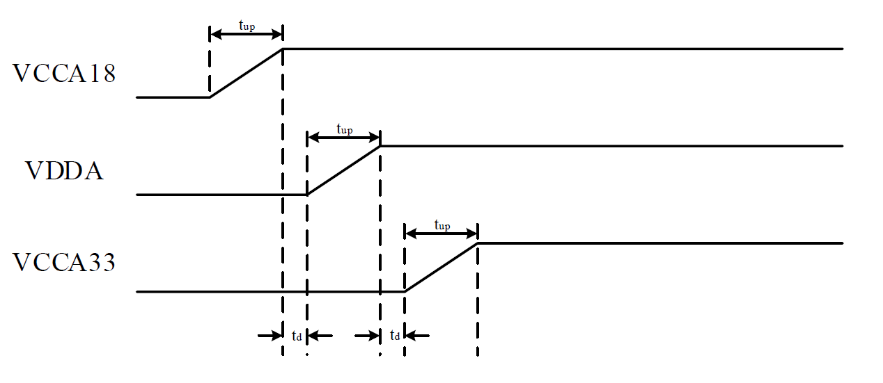
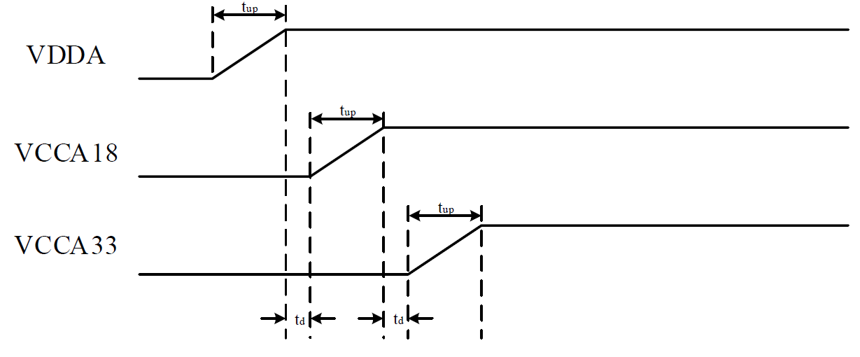
Power Up Sequence
There are three powers and they are VCCA33(3.3V)、VCCA18(1.8V) and VDDA(0.9V), IP
supports power up sequence in any combination because it has power-off protection
design between the three powers. But there is a over voltage case that 1.8V MOSFET
works under 3.3V power, the IP has breakdown voltage design to protect the 1.8V
MOSFET, but anyway we suggest to power up VCCA33(3.3V) finally for protecting the
1.8V MOSFET during the power-on period. Figure 1. USB Power Up Sequence 1Figure 2. USB Power Up Sequence 2
Table 2. USB Power Up Parameter
Name
Description
Min
Typ
Max
Unit
tup
the time of power-up
200
us
td
the delay of two power-up
>0
us
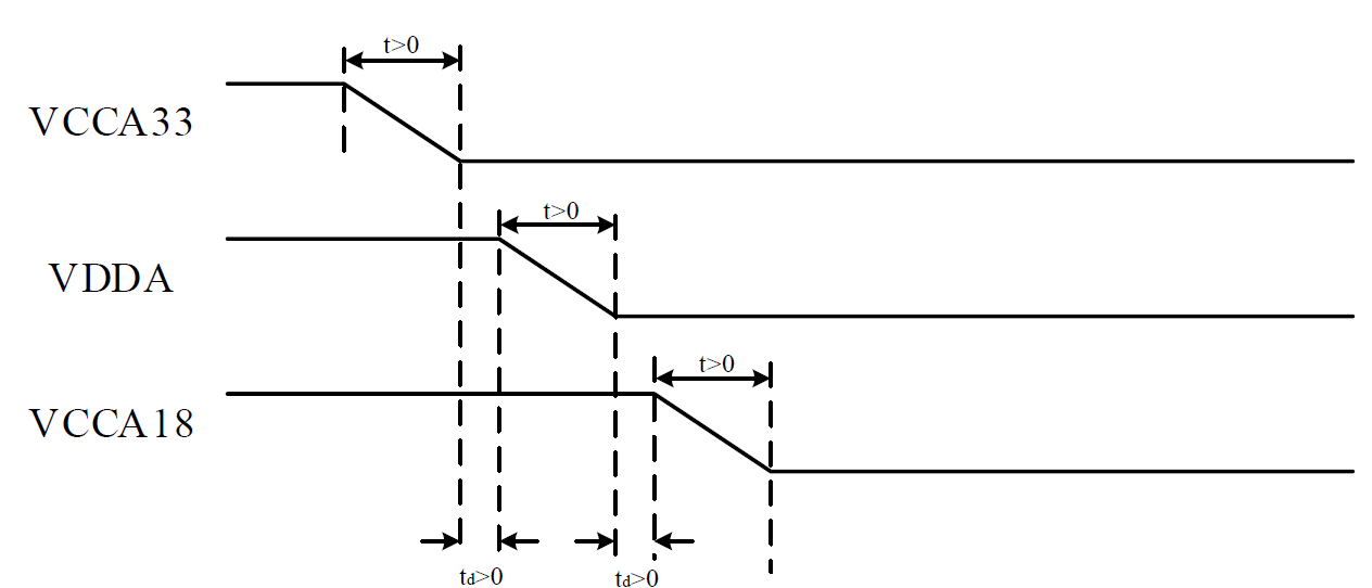
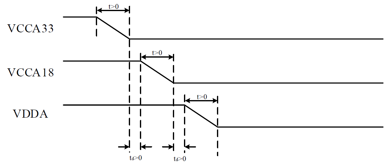
Power Down Sequence
There are three powers and they are VCCA33(3.3V)、VCCA18(1.8V) and VDDA(0.9V), IP
supports power up sequence in any combination because it has power-off protection
design between the three powers. But there is a over voltage case that 1.8V MOSFET
works under 3.3V power, the IP has breakdown voltage design to protect the 1.8V
MOSFET, but anyway we suggest to power down VCCA33(3.3V) first for protecting the
1.8V MOSFET during the power-on period. Figure 3. USB Power Down Sequence 1Figure 4. USB Power Down Sequence 2