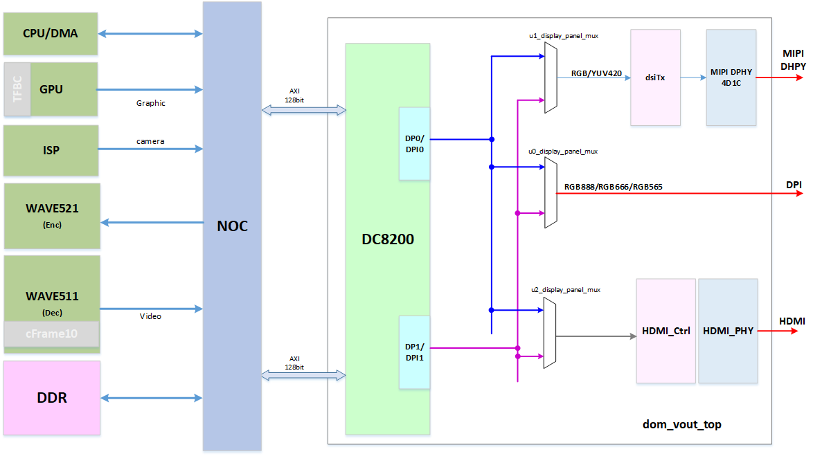
The display subsystem, named as dom_vout_top in the JH7110 system, includes
front-end video data capture, display controller and display interface, such as RGB IF,
HDMI, and MIPI.
In the display subsystem, DC8200 display controller works as a third party
high-performance optimized-area Display Processor Unit (DPU) IP that can be used for
reading rendered images from the frame buffer to the display.
Block Diagram
The block diagram shows the block diagram of the display subsystem. Figure 1. Display Subsystem Block Diagram
DC8200 Display Controller
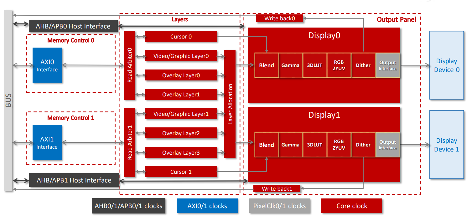
The following image shows the block diagram of the DC8200 display controller. Figure 2. DC8200 Display Controller Block Diagram
The following components are included.
Host Interface: Allows communication with the system
and the DC controller. The host interfaces include the AXI, AHB, and APB. In
this block, data crosses clock domain boundaries.
Memory Control: Contains the AXI interface to manage
the access between the system memory and layers of the DC8200.
Write Back: For debug use only.
Layers: Include video/graphic, overlay, and cursor
layers.
Video/graphic layers support both video and graphic configurations.
Video/graphic and overlay layers support dynamic layer allocation
and de-gamma.
Overlay 1 and overlay 3 do not support scaling, rotation, and line
buffers.
Cursor layers provide hardware cursor functionality.
Dither: Provides a Lookup Table
(LUT).
Gamma: Performs gamma correction.
Output Panels: Support two output panels, as shown by
Display0 and Display1.
Output Interfaces: Support parallel pixel output with
30-bit Data, Horizontal Sync, Vertical Sync, and Data Enable. Support easy
adaptation to external serialization logic, for example, HDMI.
Pixel Pipelines: Reside in the layers and output
panels. Two display pipelines support linear and tiled frame buffers for RGB
and YUV inputs. Optional enhancements include multiple overlay layers,
composition and blending, up/down scaling with multi-tap filtering, and
color space conversions.
Video Output Driver Framework
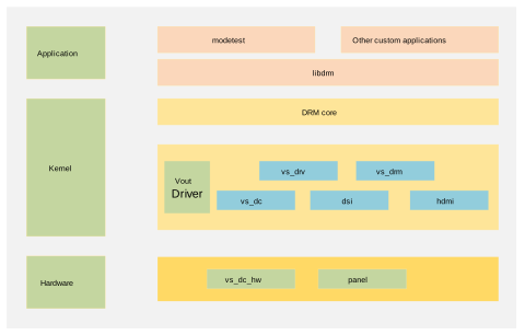
The following figure shows the framework of the video output driver and the display
controller.Figure 3. Driver Framework
The video output driver framework has the following 3 layers.
Application layer: Consists of application code and
test code and communicate with kernel layer through
libdrm.
Kernel layer: Consists of DRM
core and Vout driver. DRM
core receives commands from libdrm
and transfers to Vout driver.
Hardware layer: Connected with Vout
driver, and operates the hardware directly.
Display Subsystem Device Tree Source Code
In the jh7110.dtsi file, you can find the device tree source
code of the display subsystem as
follows:
compatible: Compatibility information, used to
associate the display controller and its target device.
dss-syscon: The SYSCON register(s) of the display
panel.
reg: Register base address
"0x29400000" and range
"0x100".
interrupts: Hardware interrupt ID.
status: The work status of the display controller
module. To enable the module, set this bit to okay or
to disable the module, set this bit to disabled.
clocks: The clocks used by the display controller
module.
clock-names: The names of the above clocks.
resets: The reset signals used by the display
controller module.
reset-names: The names of the above reset signals.
power-domains: The power supply domain of the display
controller module.
Note: Except for the status
parameter, you are not recommended to change the values of other parameters
unless you know exactly what you are doing.